Where will the high power amplifier fidelity issues get solved?

Let’s face it, the high power amplifier is not linear enough. Low power systems perform much better but when you start combining transistors to make modules, you lose fidelity. When those modules are combined for even more power, the linearity degrades further.
In this technical brief I’ll be discussing an approach and architecture that will improve linearity for solid state high power RF and microwave amplifiers by orders of magnitude, whether class A or class AB topologies, although the fundamental principles can also be applied to TWT and MPM amplifiers as well.
For certain, it will never be the RF component manufacturers who solve this problem. Linear performance is relative and it’s the low power, non-combined, RF device linearity that sets the bar for what is considered the best achievable linearity performance. However, since the high power system amplifier combines devices the system amplifier linearity will always be inferior to the individual device. In other words, the high power system amplifier will always fall well short of desired linearity, even as RF semiconductors and other components in the RF path improve.
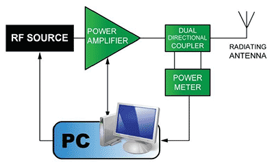
It is the system integrator that purchases the amplifier who becomes responsible for addressing the performance issues of the HPA, and they do so by designing their own control loop external to the system amplifier. Figure 1 depicts such an application where enormous effort, cost, and time is applied to designing, building, and testing the external hardware and software control loop used to level the amplifier output. This approach also requires a calibration process that the system integrator performs on each amplifier, storing "cal" factors to be applied by the external control loop for adjusting the input level.
In Figure 1 you are required to add the external feedback loop under PC control for metering, output level control and exciter control, and you might also add costly harmonic filters and switches (if you can get them at your required power levels). In some cases, multiple amplifiers are used for multi-channel operation because of poor IMD performance. It is also common to operate the amplifier at much lower than fully rated output power, thereby increasing your effective $/watt while decreasing power density.
What does the future architecture look like?


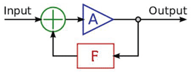
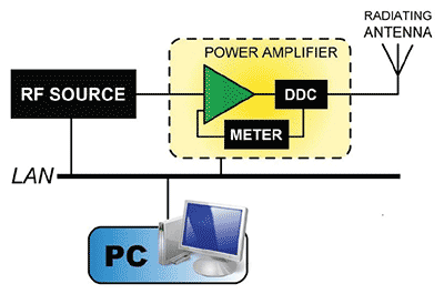
The coming architecture will be a closed loop with digital real time feedback shown in Figures 2 and 3. Ok, maybe that’s not a surprise and you likely have seen analog or digital predistortion before, but keep in mind you cannot purchase a broadband HPA with this technology today. Today, your system engineers are expected to close the loop themselves. Admittedly Figure 2 is a terrific oversimplification. In reality, the input and output signals are both digitized and the input/output inverse error function are added digitally and then converted back to RF with a DAC before the amplifier stages. But the solution is actually more complicated than that, since it includes the ability to measure and adjust the phase difference between input and output. Furthermore, the available DAC, ADC, and FPGA speeds have not been up to the task, not to mention the absence of FPGA and DSP expertise at the typical amplifier manufacturer due to lack of need..
In Figure 3 the control loop is now internal to the amplifier. The PC commands the signal source and amplifier, the amplifier reports status to the PC - the PC does no signal processing. The PC does instruct the amplifier the desired output power and the modulation scheme and does set the sig gen frequency and modulation but the sig gen output level need not be controlled or calibrated and is allowed to drift. Instead the amplifier output is precise and the amplifier is the calibrated instrument.
Is this digital predistortion?
For many of you, digital pre-distortion is something you have seen before but this is different because the predistortion I’m talking about is done on the RF signal, not the baseband of the demodulated carrier. Today’s digital predistortion is done in the baseband with the purpose of improving bit error rates on narrow band communications transmitters. In fact, you can buy the Analog Devices AD9375 to perform digital pre-distortion, albeit limited to less than 100 MHz bandwidth. The architecture I’m describing digitizes the entire RF to make a very linear broadband HPA, seen in Figure 4.

From a technology standpoint, what is needed are ADC’s and DAC’s capable of at least 6 Giga samples per second and 14 bits resolution. There are additional DSP techniques required (outside the scope of this discussion) that provide effective oversampling of a 6 GHz microwave signal. I say 6 GHz because the technology is close to becoming available and our modeling has shown with this upcoming technology, digital predistortion can linearize the entire spectrum, from DC to 6 GHz.
How far into the future?
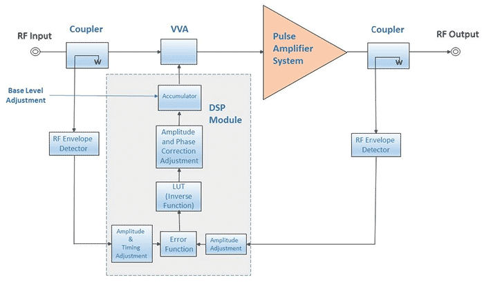
This year looks to be the watershed year with the market introduction of not only ADC’s and DAC’s with sample rates fast enough and with the required resolution, but also FPGA's with the appropriate fabric to accomplish the task. Implementing this feedback architecture in, let’s say a standard lab rack mount amplifier for product testing, is not that far away. For example, all of our new amplifiers have a feedback loop architecture that includes an FGPA. Furthermore, in Figure 5, you see the block diagram of our upcoming pulse shape matching design for which we have demonstrated the proof of concept. You will notice the lack of input digitization and the inclusion of VVA control. In this case we are correcting what is essentially AM modulation. We don’t need to measure and adjust for phase, so the digitizing and processing speeds can be accommodated by today's technology. This is the intermediate step on the way to ultra-broadband digital pre-distortion but is a complete implementation of a closed loop HPA architecture. In other words, the architecture is currently in play allowing for evolution of the function (F).

EW
A single broadband amplifier can be used to communicate in multiple channels while jamming adjacent channels, as well as transmitting a radar pulse, all simultaneously! That’s clearly a huge military advantage in capability and it comes with meaningful reduction in cost and significant size and weight reduction in total mission hardware.
Radar
How about achieving a virtual exact reproduction of the input pulse including the elimination of droop? No more tuning or tweaking the amplifier’s transient response or manipulating the input pulse. No more excessively large capacitance on the power supply to compensate for droop. The clean pulse will improve radar detection performance and, for radar threat simulation applications, allows for exact reproduction of recorded adversary radar for improved threat simulation.
Test & Measurement
With a very linear HPA, you can test with multi-tones and not have to deal with intermodulation distortion. PIM testing will also be easier to do and will have a higher dynamic range. The future architecture of the RF High Power Amplifier will also have the characteristic of being a calibrated instrument. Imagine all the product testing applications where the external DDC, power meter, and power sensors can be eliminated.
What are the implications?
Let’s take the general case of harmonic distortion where all applications benefit from improvements. Knocking down the second and third harmonics from -20 dBc to -60 dBc, for example, eliminates the need for external filtering, thereby reducing cost, weight, size and insertion loss while improving reliability. Not to be overlooked, external metering is no longer required and the amplifier becomes a calibrated instrument.
Concluding Remarks
The architecture of the future will solve the amplifier issues within the amplifier rather than rely on the system integrator to complete level control and calibration with an external loop. Costly and heavy external filters, switches and multiple narrow band amplifiers will no longer be required. New applications will be enabled with the dramatic reduction in overall system $/watt, the significant reduction of SWaP and meaningful improvement of power efficiency. And best of all, this architecture is just around the corner.
Empower RF Systems manufactures the most advanced high power system amplifiers in the world with solutions for defense, commercial, and industrial applications. Our products incorporate the latest semiconductor and power combining technologies and originate from an extensive library of "building block" designs. Solutions range from basic PA modules to multifunction PA assemblies with real time embedded microprocessor control, programmable detectors, and reconfigurable digital loop control.


